
I had one of those miniature security camera boards and wanted to use it as a video source for an FPGA project. There were pins brought out for a serial connection that would send a single still frame but would be JPEG encoded and would take about 20 seconds per frame. Way too slow for what I wanted. There was also a pin for NTSC video out. NTSC is analog, not digital, and you need to sample it at about 25 MSPS. The ADC I had on my FPGA board was rated at 1 MSPS max. Also it communicated over I2C, instead of directly presenting the resolved bits of the conversion, so this would make it that much less real time and therefore not practical. Thought I might have to order a faster ADC and wire that up to use that signal. That’s when I came across these posts by Andrew “bunnie” Huang:
I decided to take it one step further(or backwards) and try to really get it to just work with loose through-hole resistors on a breadboard. Here’s the results:
There’s some noise, it’s a little washed out, it’s only 4-bit resolution, luminance only no chroma info, But…. IT WORKS!!!! Here’s the principle on a high level. Many FPGA’s support reading differential signals, so they have the hardware to compare 2 voltages. If you create a resistor ladder, and setup differential input pairs, one for each rung of the ladder(paired with the input), then you can make a flash ADC, EVEN if you only have a breadboard and a handful of resistors(‘closely’ matched). There’s limitations like the voltage range you can read and how many pins you need, but still.
I’ve put the VHDL code I wrote at:
https://github.com/bobparadiso/DIY-FlashADC
The resistor ladder I made uses 16 resistors that are matched close enough(97-99 ohm).
I also have a POT setup which acts like a contrast control, but it’s main function is to divide the voltage so that the ladder is dividing only about 1.3V. NTSC is 1Vpp. I set the reference voltage for the ladder a little higher to increase the contrast.
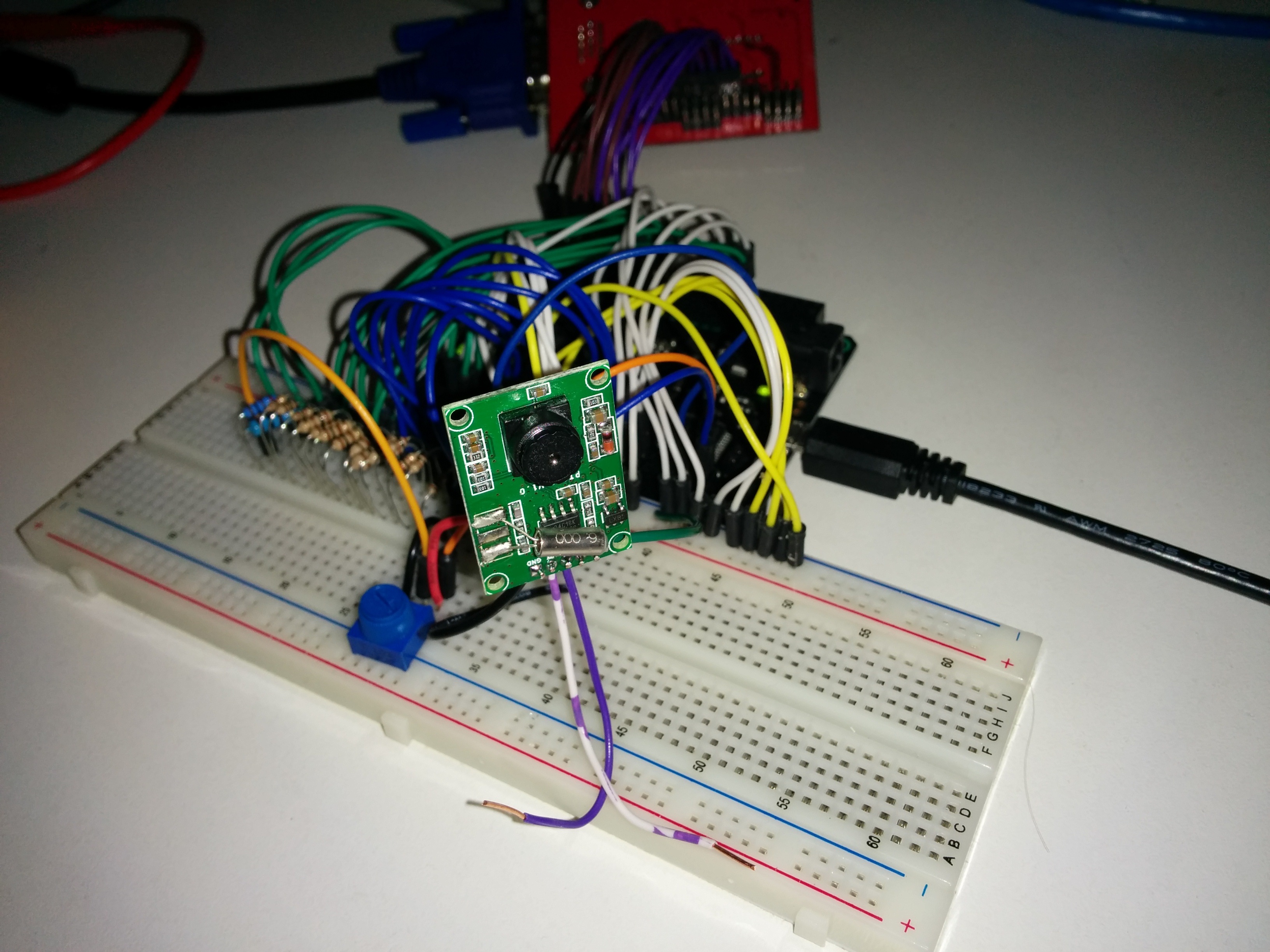
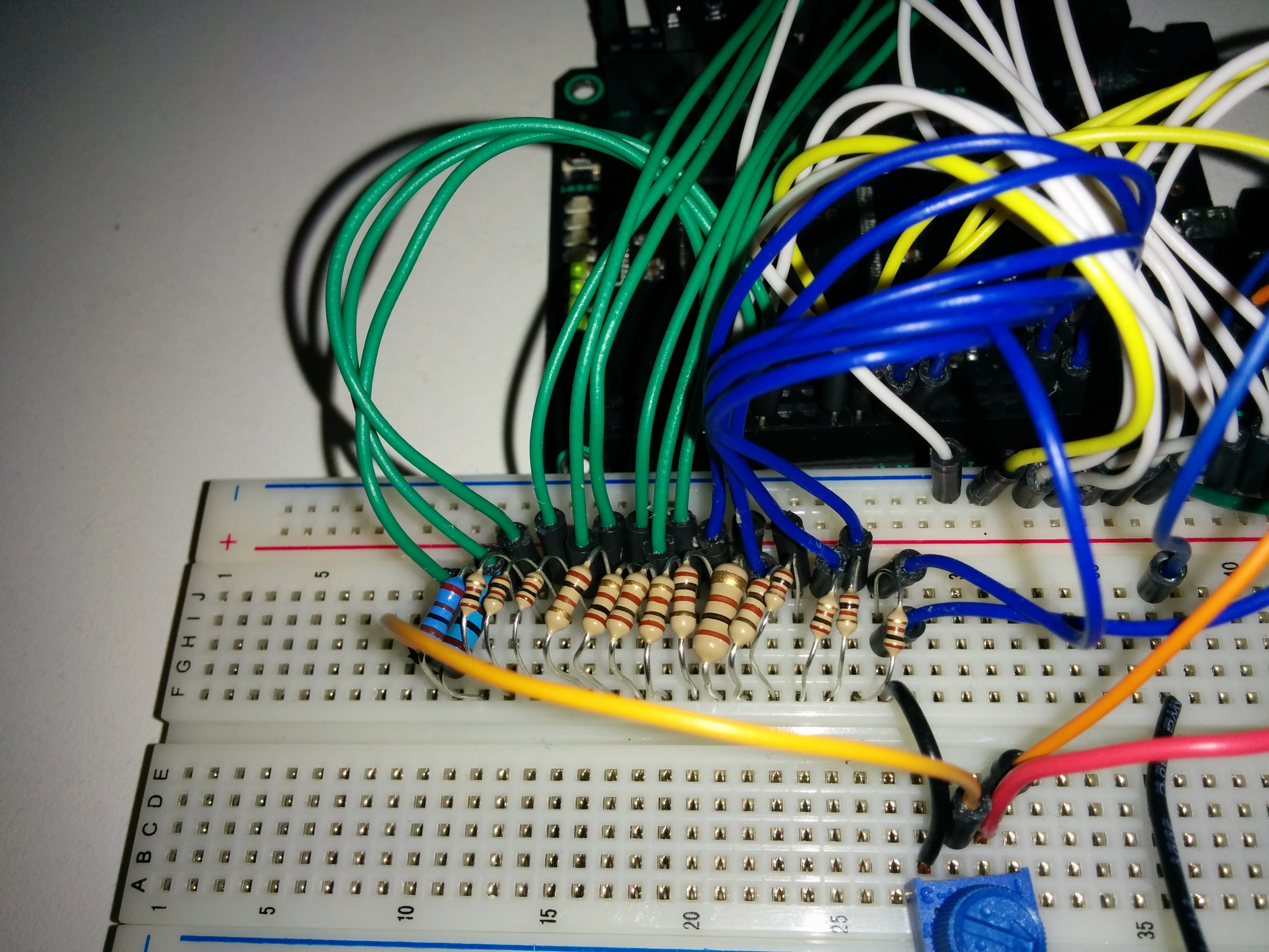
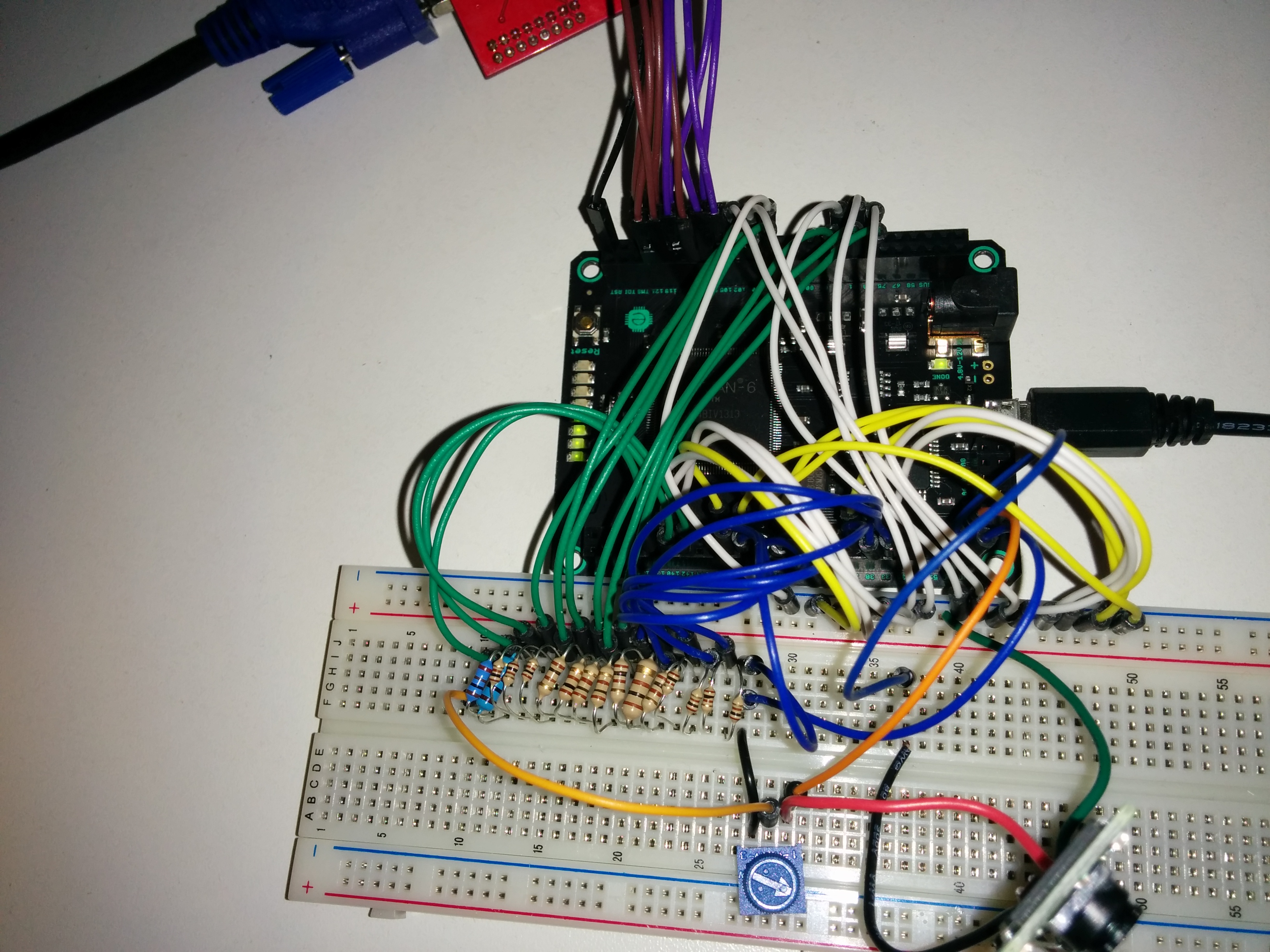
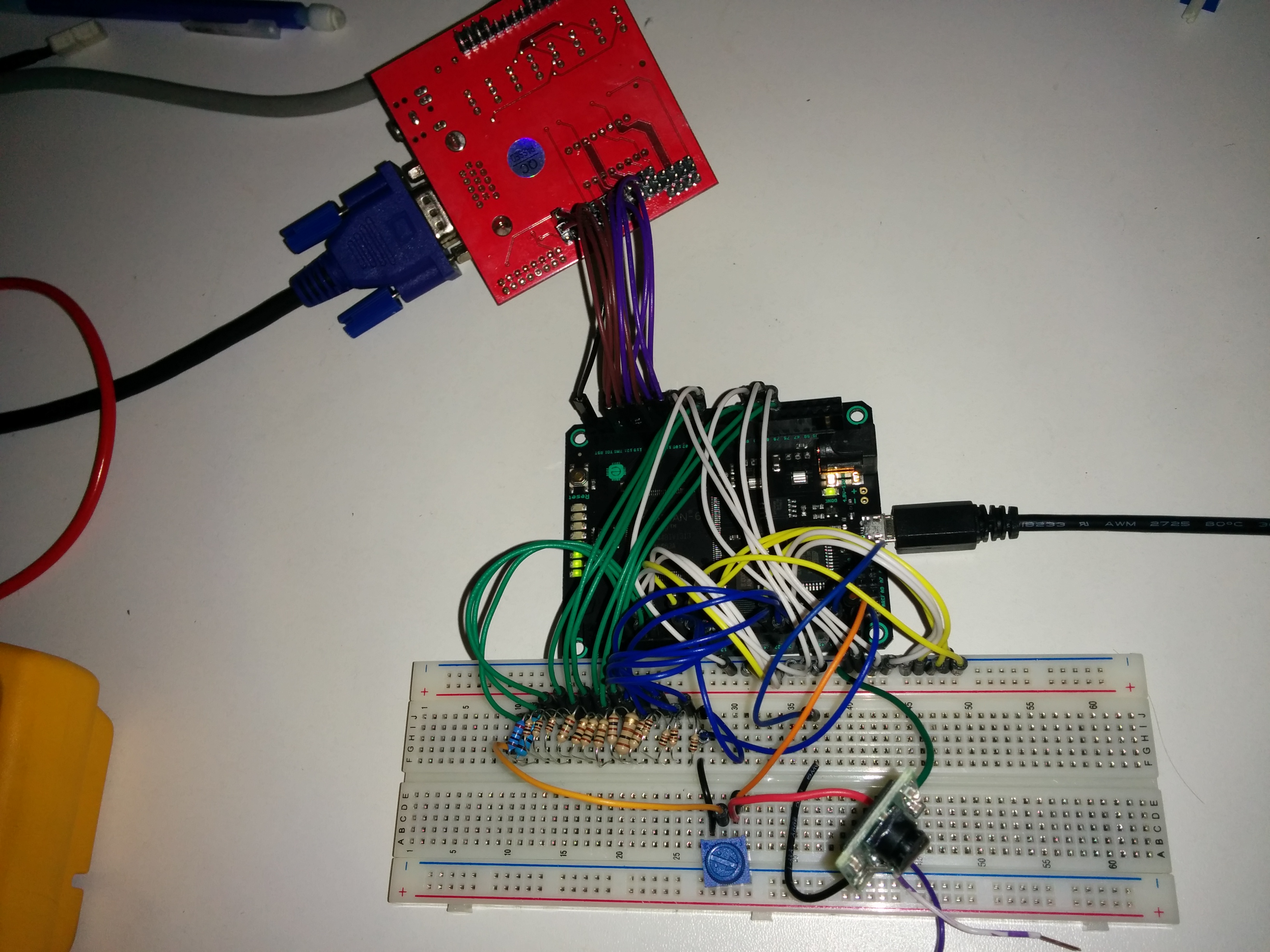
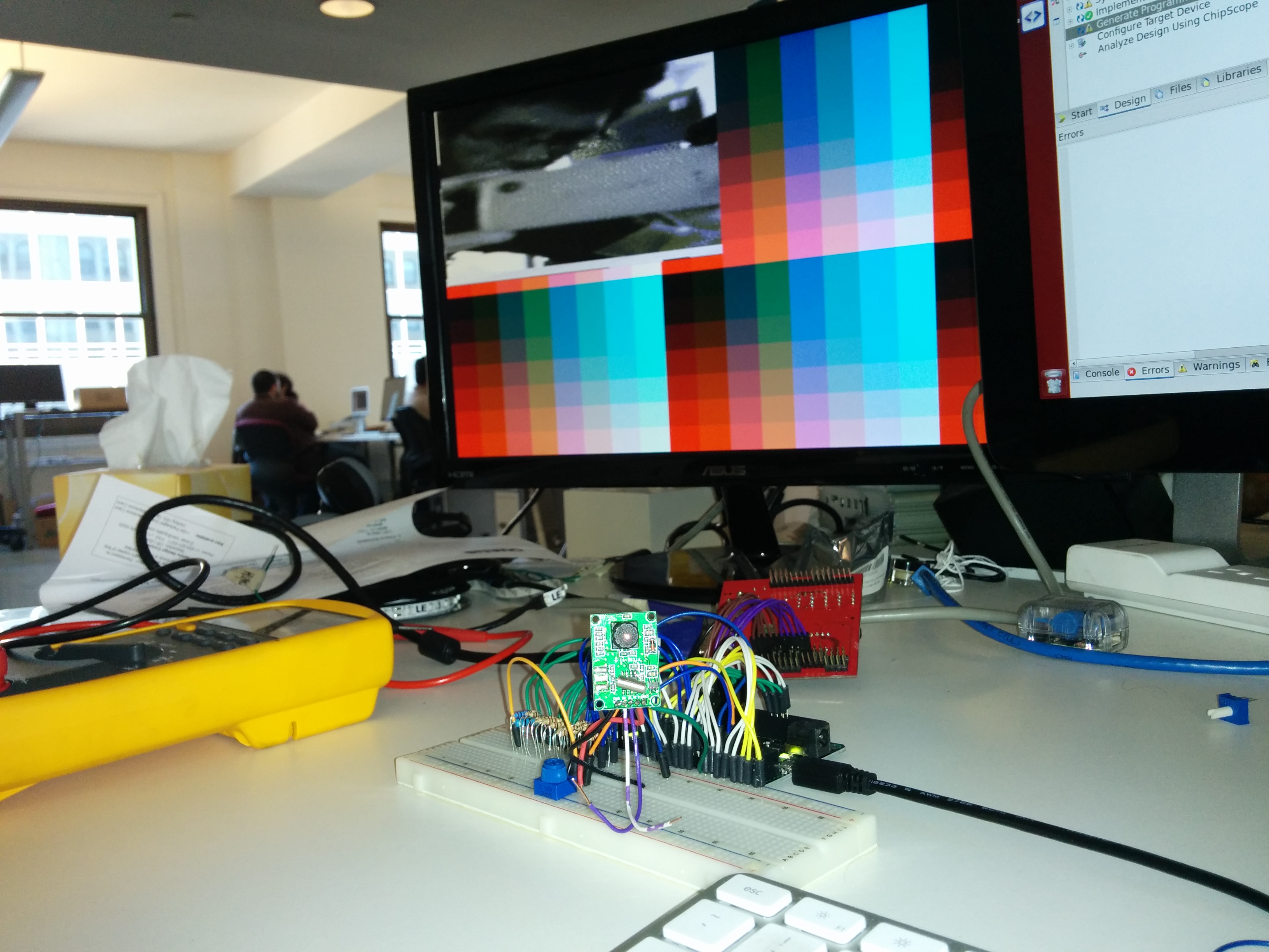
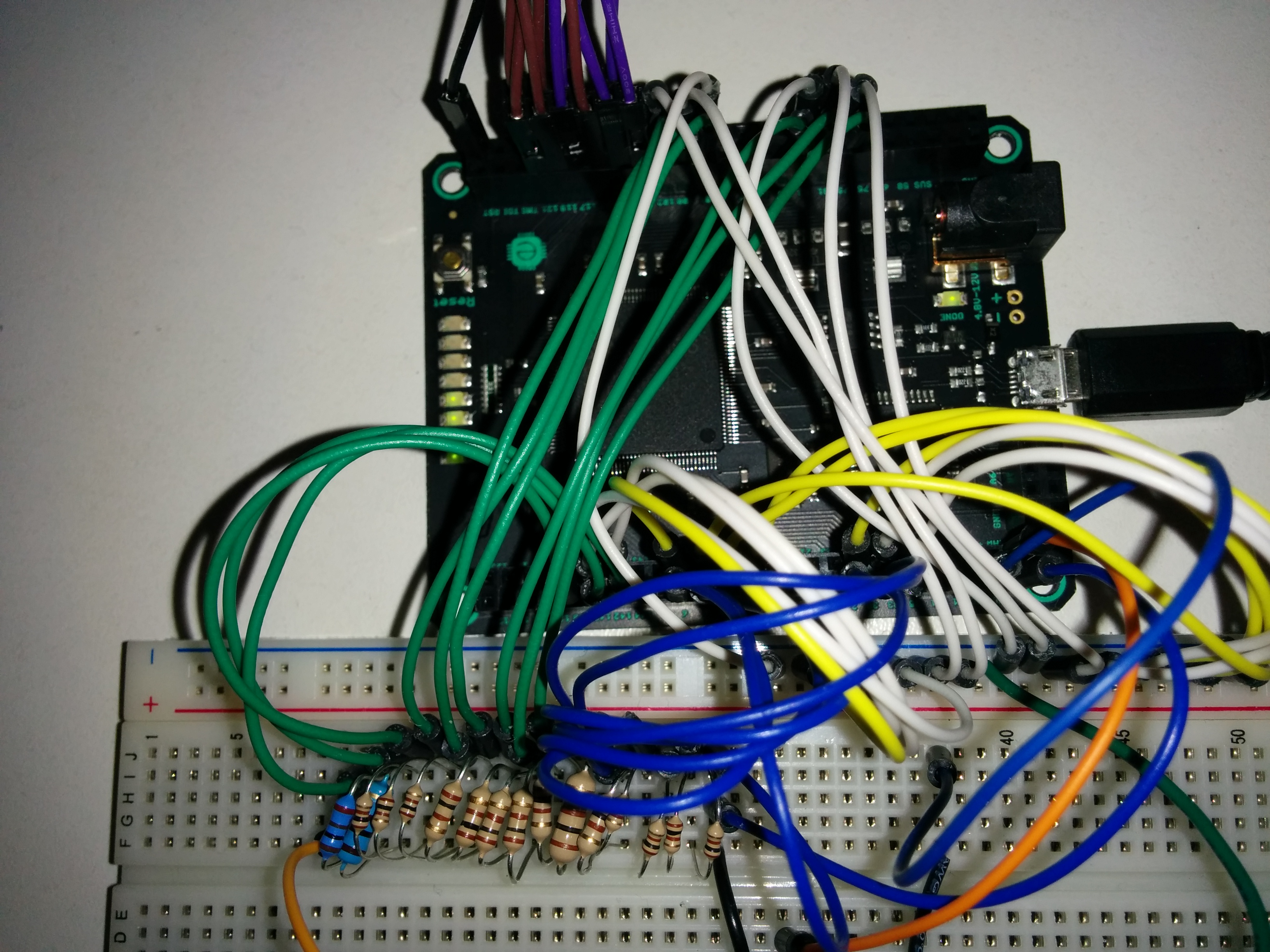
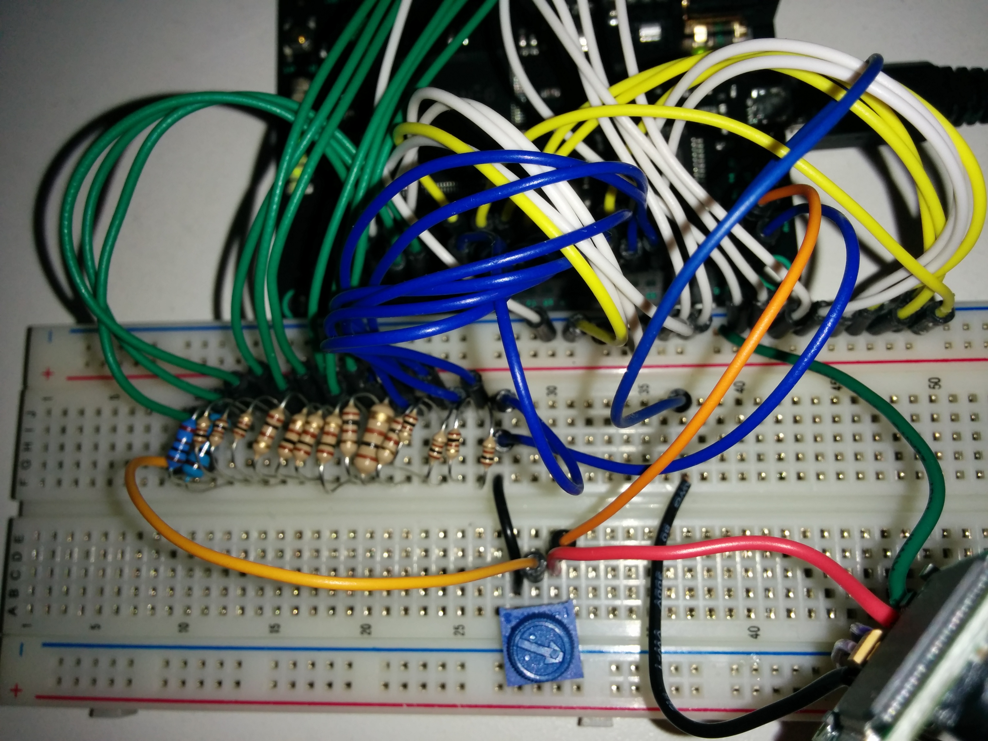
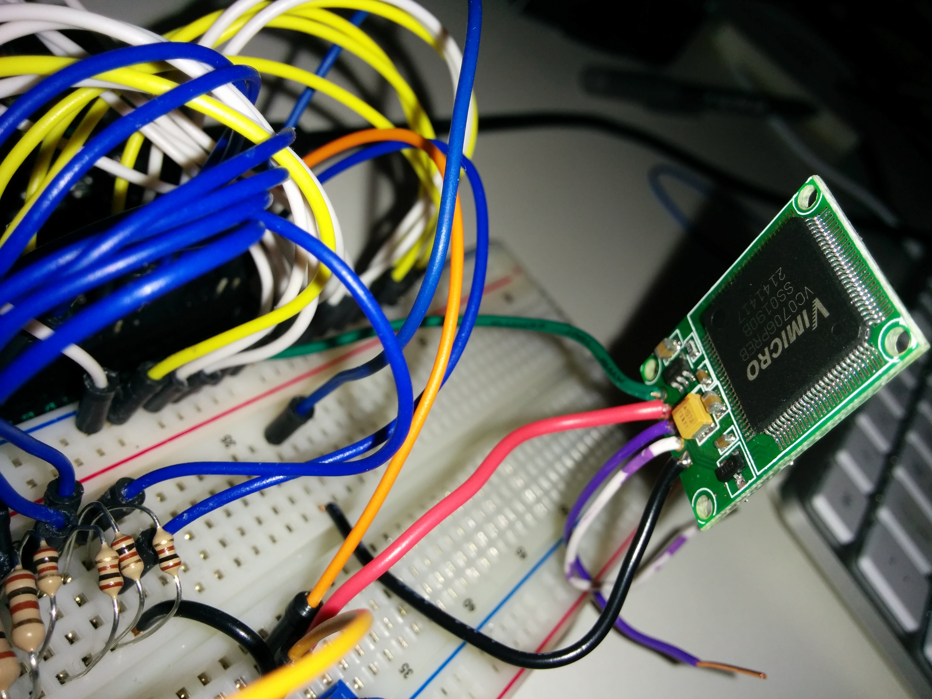
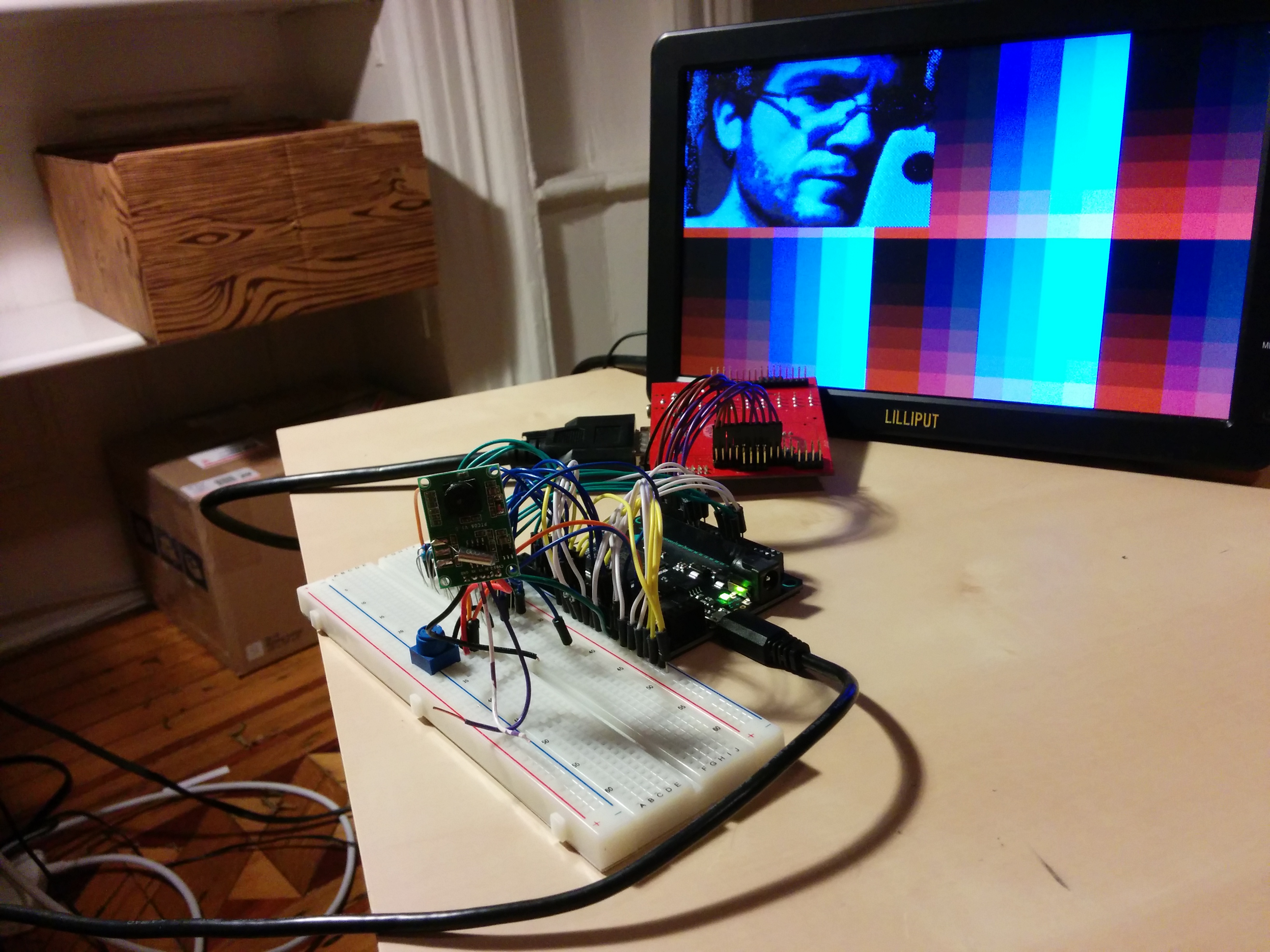
The green wire from the camera is the NTSC output. I’ve plugged that into the blue strip on my breadboard and run separate wires from that to each of the 16 differential pairs I’ve enabled on my FPGA. To each pair is also one wire going to one rung of the resistor ladder.
All in all, it’s a ‘lot’ of wires, and is not how you’d produce anything for production. BUT, the fact that you ‘can’ do it this way is awesome and very instructive. I certainly learned a lot working on this. And who knows, you might be in a pinch someday and could use something like this for a relatively high speed but lower precision ADC.
Special thanks again to Andrew “bunnie” Huang!
